BACK-END · MEMORY
Memory Layout
Compact, reliable SRAM and register-file layout engineered for yield.
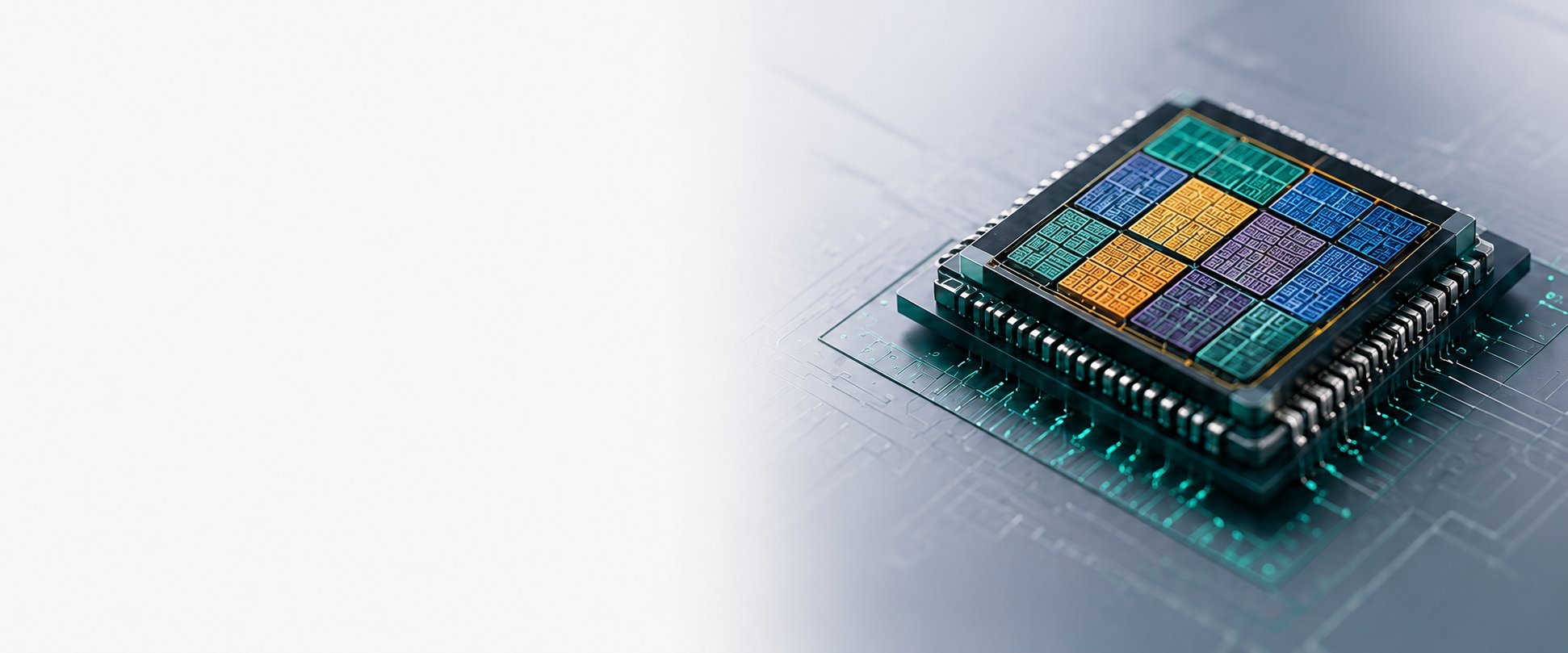
Compact, reliable SRAM and register-file layout engineered for yield.
Memory arrays are usually the densest, most yield-sensitive part of a design. We build SRAM bit-cell and register-file layout engineered for density and manufacturability at your target process node, with repair and redundancy structures built in where they're needed.
Compact, DRC-clean bit-cell layout optimized for your process node.
Dense, timing-aware register-file layout for embedded memory blocks.
Configuration and validation support for memory compiler-generated arrays.
Layout compaction strategies balanced against manufacturing yield data.
Layout for redundant rows/columns and built-in repair logic.
Full design-rule and LVS closure specific to dense memory layouts.
Layout support for high-bandwidth, 3D-stacked memory architectures.
Higher density with optimal array layout.
Timing and power-aware design approach.
DFM-driven layout for better manufacturability.
Proven across advanced process technologies.
Validated across production tape-outs.
Share your spec, node, and timeline — we'll scope exactly what it takes.