BACK-END · LAYOUT
Physical Layout
Full-custom and standard-cell layout built to close DRC/LVS on the first pass.
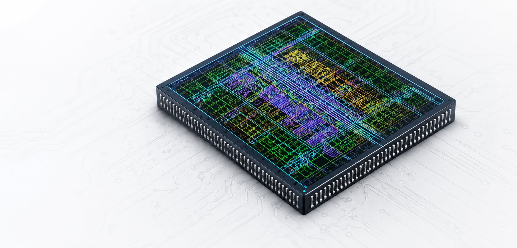
Full-custom and standard-cell layout built to close DRC/LVS on the first pass.
Layout is where micron-level decisions determine yield and manufacturability. Our physical layout team delivers standard-cell and full-custom layout engineered to close design-rule and LVS checks cleanly at your target node, with parasitics accounted for from the start.
Cell-level layout optimized for density and characterization consistency.
Hand-crafted layout for blocks where automated placement falls short of spec.
Systematic design-rule and layout-versus-schematic resolution ahead of sign-off.
Layout structured for accurate RC extraction and post-layout correlation.
Full LVS closure against the reference schematic before hand-off.
Fast-turnaround layout edits for late-stage engineering change orders.
Layout decisions co-optimized with process and device characteristics at advanced nodes.
Methodology and checks built to close DRC/LVS on the first pass.
Yield-driven layout with smart density and OPC considerations.
Experienced across 7nm to 2nm and beyond technology nodes.
Optimized flows and ECO strategies for faster delivery.
Robust verification and sign-off for reliable tape-outs.
Share your spec, node, and timeline — we'll scope exactly what it takes.