BACK-END · PD
Physical Design
Floorplan, place and route tuned to the PPA targets your product actually needs.
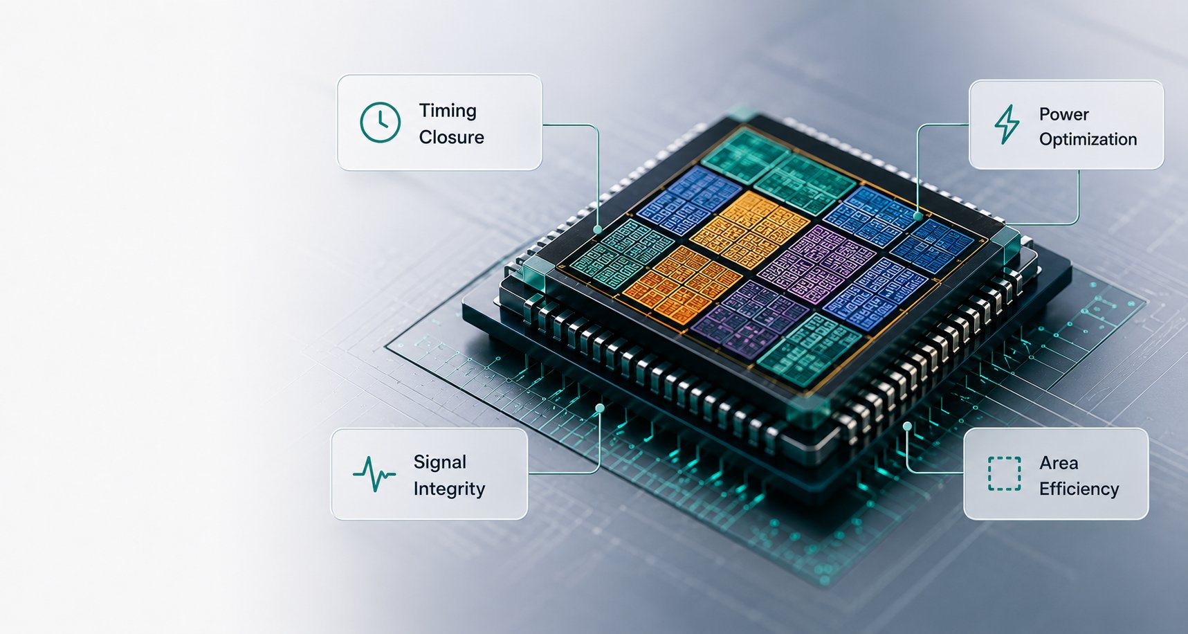
Floorplan, place and route tuned to the PPA targets your product actually needs.
Physical design is where architectural intent either survives contact with silicon or doesn't. We take your netlist through floorplanning, placement, clock tree synthesis and routing with your specific power, performance and area targets driving every decision — not generic default flows.
Block placement, power grid design and macro planning for routability and IR-drop margin.
Timing-driven placement and low-skew CTS tuned to your frequency targets.
Detailed routing with DRC-aware optimization ahead of sign-off.
Multi-corner, multi-mode STA with systematic closure across setup and hold.
Dynamic and static power analysis with IR-drop and electromigration checks.
Final timing, power and physical sign-off documentation ready for tape-out.
Floorplanning and interface design for 2.5D/3D advanced packaging and chiplet-to-chiplet integration.
Every decision driven by performance, power and area.
Methodologies that scale across complex SoCs.
Robust verification for first-pass silicon success.
Optimized flows and automation for faster turnaround.
Final documentation ready for hand-off.
Share your spec, node, and timeline — we'll scope exactly what it takes.